 Fraunhofer Institute for Biomedical Engineering
Technologies
Common silicon-based MEMS technologies like photolithography, wet and plasma etching, deposition of dielectric and metallic layers (PECVD, sputtering, evaporation) and anodic bonding.

© Fraunhofer IBMT.
Common silicon-based MEMS technologies like photolithography, wet and plasma etching, deposition of dielectric and metallic layers (PECVD, sputtering, evaporation) and anodic bonding.
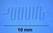
Dry film resists as functional layers for microfluidic systems. Films can be applied on polymer, glass or silicon substrates. The height of microfluidic channels can be varied by stacking of several films.
SU-8 photoresist can be used as an alternative to dry film resists, if high lateral resolution is required. Covering of microfluidic channels will be done by bonding of glass chips already containing holes for fluidic access or by laminating of a cover foil.
PDMS casting can be used for replication of components in small numbers. Extensive experience in both casting and mould-making is available.
A roll-to-roll hot embossing process is available for mass production of (fluidic) micro structures in large area polymer foils (COC, PC, PMMA, PS etc.). Even structures in the sub-µm range can be replicated by this process. A possible application of sub-µm structures is influencing cell behaviour (e. g. reduced cell adhesion) on large-area substrates.
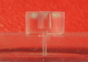
Several concepts are available for realizing fluidic interfaces to the user. One approach is using PDMS casting to realize a septum which is combined with the microfluidic system. This septum provides a simple port for sample injection and is self-sealing after retention of the cannula. Thus, it additionally provides the functionality of a valve.
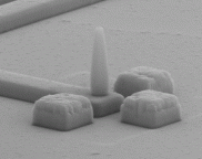
Rapid prototyping of real three dimensional polymer structures with sub-µm resolution. This is achieved by using the multiphoton-effect for patterning photosensitive polymers like SU-8 photo resist.
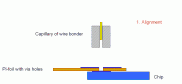
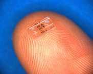
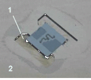
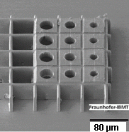
The MicroFlex-Technology facilitates the interconnection of microdevices with an ultra-thin, lightweight and highly flexible flat ribbon cable. Multilayered and shielded tracks of >10 µm and a bending radius of 100 µm are possible.
Deposition of hydrophobic, humidity non-permeable Parylene Layers
e. g. for encapsulation of electronic circuitries.